Surface Analysis and Material Characterization Consulting
Thomas F. Fister, Ph.D.
X-Ray Photoelectron Spectroscopy (XPS)
or
Electron Spectroscopy for Chemical Analysis (ESCA)
In a Nutshell
Take Home Point:
Chemical state information of sample surfaces
What It Provides:
Provides elemental surface composition/concentration and chemical state information down to sub-percent levels. Can also provide depth profiles down to a few microns via ion beam sputtering. Shallow depth distribution is possible without sputtering (i.e. no sputter-induced damage) using angle-resolved analysis. Can also provide elemental and chemical state images.
Brief Description:
X-Rays In/Electrons Out
XPS stands out from other elemental analysis techniques in that it provides detailed chemical state information (e.g. N is present as organic N, NH4, NO2, NO3 etc...) as well. In XPS, samples are exposed to an X-ray beam which causes photoelectrons to be emitted from the core levels of the constituent atoms. The energy of the photoelectrons is dependent on the particular type of atom from which it is generated. Further, the energy is affected by the chemical environment of the atoms. In general, only photoelectrons generated within the top ~10nm of the sample surface escape without losing energy resulting in XPS being a surface analysis technique. However, XPS instruments are equipped with ion guns to sputter material from the sample allowing depth profiles to be obtained. XPS can easily analyze non-conducting samples such as ceramics and plastics in addition to conducting samples (e.g. metals, alloys).
What is Detected:
Li-U
Detection Limits:
~0.01-1 Atomic % (Z Dependent)
Information Depth:
~5-7.5um
Spot Size:
~7.5-10um (smallest)
~1-2mm (largest)
Applications:
-
Surface contamination studies
-
Analysis of stains/discolorations on surfaces
-
Analysis of polymer surfaces before and after plasma treatment
-
Quality control of medical device surfaces
-
Delamination studies to reveal species responsible for failure
-
Depth profiling for surface to bulk distribution of contaminant and matrix species
-
Angle-Resolved analysis of self assembled monolayers and plasma treated polymers
-
Analysis of wear-resistant coatings in a variety of industries (e.g. consumer products, automotive engines)
Manufacturers:
1. Kratos
Greater Detail
History
In 1887 the German physicist Heinrich Rudolph Hertz discovered the ‘Photoelectric Effect’ in which electrons are emitted from materials exposed to light. However, it wasn’t until 1905 that this effect was finally understood and explained by Albert Einstein. Two years later P.D. Innes created an instrument that many consider the first XPS in which he recorded broad bands of emitted electrons as a function of velocity. In 1954 the Swedish physicist Kai Siegbahn further refined the design of Innes and following researchers to produce an instrument capable of recording high energy resolution spectra. In 1967 Siegbahn published an XPS study which opened the eyes of others to the vast potential of this technique. Later, in 1969 he collaborated with a group of engineers at Hewlett Packard to produce the first commercial, monochromatic XPS tool. In 1981 he was awarded the Nobel Prize in Physics for his pioneering work in XPS.
Process
XPS (X-Ray Photoelectron Spectroscopy) and ESCA (Electron Spectroscopy for Chemical Analyses) are the same technique. The former terminology is most descriptive to the actual physical process of the technique and is used more frequently by those in industry. The latter terminology, on the other hand, describes an important objective of the technique and is somewhat more common in academia.
As mentioned, XPS is the most descriptive to the actual process that occurs within the instrument whereby which samples are hit with a beam of X-rays causing photoelectrons to be ejected. The photoelectron energies are characteristic of the atoms from which they are generated. However, due to the short mean free path of electrons, the average distance in which an electron will travel before undergoing an inelastic collision and losing a portion of its energy, only those generated within the top surface (primarily ~50-70A) will originate from the sample without losing energy in the process. This phenomenon is what makes XPS a ‘Surface Analysis’ technique. Further, the chemical environment can slightly alter the photoelectron energy. Thus, the technique provides both elemental information (can detect all elements except for H and He) AND chemical state information (e.g. N is present as NH4, NO2, NO3, Amine etc…) of sample surfaces with detection limits in the sub-atomic percent range. The ability to provide chemical state information is a very valuable feature of XPS that sets it apart from many other material characterization techniques.
Surface analysis is important because it’s the sample surface that comes in direct contact with the environment and/or other materials. Surface composition significantly affects important properties such as adhesion, wettability, corrosion, reactivity, toxicity and failure mechanisms. However, XPS is not limited exclusively to surface analysis. It can also provide depth profiles down to a few microns via ion beam sputtering. Shallow depth distribution is possible without sputtering using angle-resolved analysis. Both of these are discussed further below.
XPS involves a photoemission process in which a sample is hit with X-rays of sufficient energy resulting in their absorption by sample atoms. This absorption process causes the emission of core level electrons termed photoelectrons. Since the photon energy is known, measuring the photoelectron kinetic energies allows the electron binding energies to be calculated by the following equation:
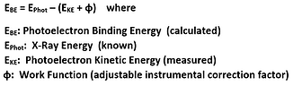
Calculating the photoelectron binding energies (BEs) allows the surface atoms comprising the sample to be determined because the BEs depend on:
The elements from which the electrons are emitted
The orbitals from which the electrons are ejected
The chemical environment of the atom from which the electrons are emitted
The energy levels of electron orbitals (e.g. 1s, 2s, 2p, 3s, 3p, 3d etc…) are distinct for specific types of atoms. For example, the 1s energy level for Na differs from that of Si. Such differences allow XPS to easily identify the elements present at the sample surface.
Each orbital within an atom exists at different energy levels. For example, the electrons within the 2s orbital of Si are more tightly bound (i.e. will have a higher binding energy) than those within the 2p orbital. Thus, for many elements multiple signals are observed in the XPS spectra and they are identified as the orbital from which they originated (e.g. Cu2s, Cu2p3/2, Cu2p1/2, Cu3s, Cu3p and Cu3d for Cu). However, typically one signal will be more intense than the others and that one is most commonly used for analysis (e.g. Cu2p3 in the case of Cu) unless interferences require the use of a secondary signal from that element.
Finally, the energy of orbitals within an atom are affected by its chemical environment. Factors affecting the chemical environment of an atom include the electronegativity of its nearest neighbor and the number of substituents. Bonding hybridization (i.e. where atomic orbitals fuse to form newly hybridized orbitals such as sp3, sp2 and sp1 in methane, ethylene and acetylene, respectively) between the nearest or next nearest neighbor also plays a role.
Once a photoelectron is ejected from an atom it now exists in an excited state as an ion. The ion can undergo one of two processes to ‘relax’ and remove the excess energy. In one process, an electron from an outer shell drops down into the hole created following the emission of the photoelectron and an X-ray is emitted. This process is of no practical interest when interpreting XPS spectra. In the other process, an outer shell electron still drops down into the hole, but rather than the emission of an X-ray, another electron from an outer shell absorbs the energy difference allowing it to be emitted. This emitted electron is an Auger electron and it has similar kinetic energies to that of photoelectrons allowing it to be detected and appear in XPS spectra. The Auger process has a higher probability of occurring for low Z elements while X-ray emission is more prevalent for high Z elements.
Auger electrons are named in a manner that identifies the 3 orbitals involved in the process:
Atom [ABC]
A: Level of initial core hole caused by photoemission
B: The Outer Level from which the hole (in Level A) is filled
C: The Outer Level from which the Auger electron is emitted
The Auger process is denoted with different orbital nomenclature from that used in XPS. Specifically, 1s is the K energy level, 2s and 2p are the L energy levels while 3s, 3p and 3d are the M energy levels. For example, common Auger signals for Na, Ti and Ga are Na KLL, Ti LMM and Ga LMM, respectively. Auger signals typically are broader and more complex than photoemission signals because different valence levels are involved in the process and secondary effects exist. However, since the process involves outer shells (i.e. valence electrons) Auger electrons are also sensitive to chemical bonding and will also undergo slight kinetic energy shifts from that of the pure element when formed in compounds.
Data
There are 3 basic types of data that XPS instruments provide. They are:
1. Spectra
2. Depth Profiles
3. Maps/Images
Spectra
XPS spectra are plots of the Photoelectron Intensity (Y-axis; plotted in ‘Arbitrary Units’) versus Binding Energy (X-axis, plotted in eV). In XPS spectra the energy axis is inversed (i.e. higher binding energies on the left side) so that it is representative of the atomic structure in which approaching the nucleus (i.e. the origin) results in a higher binding energy of the electrons.
Two type of XPS spectra exist, Survey and High Energy Resolution Spectra. Survey spectra are typically run first acquiring data over a wide energy range (e.g. 0-1400eV when using an Al Kα X-ray source). Such spectra contain all the detectable electron signals generated during XPS and are used to determine the surface species present. Each detectable element appears as a set of peaks corresponding to characteristic binding energies related to the electron configuration (i.e. orbitals) of the electrons within the atoms present within the sample. Additionally, Auger electrons of the elements present are observed.
For example, in the XPS survey spectrum for TiO2 numerous signals for Ti are observed corresponding to photoelectrons generated from the 2s, 2p, 3s and 3p energy orbitals. Insufficient X-ray energy exists to remove electrons from the 1s orbital. The Ti2p signal is the most intense and that is the one most commonly used for quantification and chemical state determination. It is also noted that the Ti2p signal actually exists as two peaks rather than one due to spin-orbit interaction which causes a shift in the atomic energy levels of the p orbitals due to an electromagnetic interaction between the electron’s spin and the nucleus’ electric field through which it moves. Such splitting occurs in the p (as p3/2 and p1/2), d (as d5/2 and d3/2) and f (as f7/2 and f5/2) energy levels, but not the s energy levels. The magnitude of spin-orbit splitting increases with atomic number (Z) but decreases with distance from the nucleus due to increased nuclear shielding. Also observed in the TiO2 spectrum are O1s and O2s signals due to the presence of O and a C1s signal due to carbon surface contamination. Carbon contamination is almost always detected in XPS surface analysis unless the sample has been specially prepared to prevent its presence.
A high background is typically observed in survey spectra that decreases with decreasing binding energy. The background is formed by the detection of inelastically scattered electrons which lose energy during the scattering events. Because there is a high probability of inelastic scatter, many photoelectrons will be formed but lose various amounts of energy as they escape the sample resulting in higher levels of background on the high BE (i.e. low KE) side of the spectra.
As mentioned earlier, Auger electrons are also commonly observed in XPS spectra. The kinetic energy of the Auger electron is determined by the binding energies of all three electrons participating in the process.
However, the Auger Electron kinetic energy is independent from the energy of the incident photon. As such, Auger electron signals appear at different positions on the XPS Binding Energy plot when different X-ray sources are used.
Shake-Up lines are another set of features commonly observed in XPS spectra. This occurs when photoelectrons are generated from ions in the excited state rather than the more common ground state. This occurrence results in photoelectrons with lower kinetic energies (i.e. higher binding energies) corresponding to the difference in the kinetic energy between the ground and excited states. This difference is typically a few electron volts. In some systems this extra ‘satellite’ peak is relatively small compared to the main photoelectron signal (e.g. the bond shake-up satellite for C1s in polystyrene). In other systems, the satellite peak can be relatively large (e.g. shake-up lines for Cu2p in Cu compounds).
Energy loss lines are also observed in XPS spectra and result from the interaction of the photoelectron with other electrons within the sample surface region. These are most pronounced in metals (in particular the alkali and alkaline-earth metals) with the photoelectrons experiencing energy loss to the conduction electrons in well-defined quanta characteristic of each metal. The signals produced are called ‘plasmons’ with the energy between the primary and loss peak named the plasmon energy.
Relatively low intensity valence bands are commonly observed in the low binding energy region (0-35eV) of the spectra. Valence bands are caused by photoemission from molecular orbitals and from solid state energy bands. Valence band spectra provide information on the density and occupancy of electronic states in the valence band of material and can sometimes be used to help identify and/or confirm the presence of specific types of materials. However, when valence band is of specific interest, Ultraviolet Photoelectron Spectroscopy (UPS) is a better option for their analysis as it has much better energy resolution and a higher flux resulting in greater signal intensity than obtained via XPS.
Following acquisition of Survey Spectra, High Energy Resolution Spectra are acquired from specific regions in the Survey Spectrum corresponding with signals of interest. These spectra are acquired using smaller pass energies (discussed below) than that of Survey Spectra which increases the energy resolution allowing for the observation of finer binding energy details. High Energy Resolution Spectra are typically necessary to determine which chemical states exist for each detected element. For example, high energy resolution of surface carbon contamination reveals that C is often present in multiple chemical states (e.g. C-C/C-H, C-O/C-N, C=O, O-C=O) which are clearly distinguishable by distinct signals not observed in the survey spectrum.
Depth Profiles
While surface analysis is advantageous there are many times when obtaining the composition below the surface is of interest. XPS can achieve this destructively via depth profiling in which elemental composition is determined as a function of depth. This is accomplished through sequential steps of data acquisition and sputtering using ion milling. This process not only provides depth profiles showing concentrations versus depth, but can also show how elemental chemistry changes with depth. However, both composition and chemistry can be altered by the sputtering process through sputter induced damage. Thus, care must be exercised when interpreting sputtered data.
An Argon ion gun is the most common XPS sputter source. This monoatomic ion source has been used historically for depth profiling on both XPS and AES instruments. This ion source is well suited for profiling hard materials (e.g. metals, inorganics, ceramics etc…), but their use in profiling soft materials (e.g. polymers, organic films etc…) have significant limitations as they damage these materials and alter their chemistry. Some instrument manufacturers now also offer C60 and Ar cluster ion sources as alternative options for profiling soft materials. These guns use a large and heavy ion for sputtering. The single charge is spread over the entire ion resulting in much less energy being transferred to the sample at the point of impact. Thus, less damage occurs and profiles of soft materials tend to maintain their chemistry through the profile. It should be noted, though, that these alternative ion sources do not efficiently sputter hard materials.
Shallow depth information can also be obtained nondestructively without sputtering using a technique called angle-resolved XPS (ARXPS) analysis. Here the sample is tilted at selected angles with respect to the analyzer. The angle determines the sampling depth with shallow and large angles resulting in smaller and larger information depths, respectively. The sampling depth (d) is approximately equal to 3λsinθ where λ is the Attenuation Length and θ is the angle between the sample and the analyzer (i.e. Take-Off Angle or TOA). Thus, by varying the TOA, one is able to vary the sampling depth allowing the user to determine which species may be predominantly at the surface and which may be localized at deeper levels. This type of analysis is only useful for films thinner than about 12nm, typical XPS information depths. However, the actual depth varies depending on the material being analyzed and the X-rays being used.
Some instrument manufacturers use a slight variation of the ARXPS process described above. Rather than obtaining individual spectra acquired at different TOAs by physically moving the sample, a process called Parallel ARXPS is used. Here the sample is NOT tilted. Instead the radian lens spectrometer provides energy dispersion in one direction and angular dispersion in another direction on a 2D detector. Both are collected simultaneously and data is collected over a range of 60o with an angular resolution of 1o. Each acquisition produces data from 60 different angles. From this data Relative Depth Plots can be constructed which show the relative positions (NOT thickness or depth) of species present in the information depth. Alternatively, ultrathin depth profiles can be extracted from the data using mathematical algorithms involving Maximum Entropy. However, information on the film (e.g. approximate composition and thickness) is needed to obtain best results for this depth profile extraction.
XPS also can determine film thickness of ultrathin films by comparing the intensity of photoelectron signals unique to the overlayer to that from signals unique to the layer beneath. This is done using the following formula with the thickness of SiO2 on Si used as an example

Mapping/Imaging
Mapping and Imaging can be used in XPS to determine whether compositional uniformity or localization of species exist on sample surfaces. In addition to providing elemental maps/images like AES, XPS can also provide chemical state images. This type of imaging is unique to XPS.
The various XPS manufacturers take different approaches to mapping/imaging. For instance, one rasters the X-ray source across the stationary sample surface with data being collected from each spot. The image resolution is dependent on the spot size of the X-ray beam (down to ~7um). This mode is known as mapping. Other manufacturers scan the stage with the X-ray source remaining fixed and utilizes apertures in the spectrometer to define the analysis area. This mapping mode achieves image resolutions down to ~15um but can image much larger fields of view (e.g. 70mm x 70mm). These same manufactures also utilize Parallel Imaging. Here the spatial orientation of the photoelectrons are maintained as they traverse the system onto a 2D detector. This mode of operation is much faster than mapping and can achieve resolutions down to ~1um. However, only a single energy is imaged. Obtaining spectra at each pixel requires acquiring images at a series of binding energies encompassing the energy window of interest.
Samples
Unlike AES, XPS can analyze insulating as well as conducting samples. No additional sample prep is necessary. This is because XPS involves bombarding the sample with X-rays which have no charge, unlike AES and SEM which utilize a beam of electrons. The emission of photoelectrons and other species can result in some sample charging but this is typically sufficiently compensated with electron and ion flood guns.
The major limitation with XPS hinges on the fact that it is a high vacuum technique. Thus, samples must be vacuum stable and fit inside the vacuum chamber. Samples that heavily outgas can cause problems in vacuum instruments. All modern XPS instruments can handle samples that are smaller than 60mm in diameter and 20mm in height. Some manufacturers offer larger analysis chamber options that can hold larger samples (e.g. 200mm wafer) as well.
XPS analysis areas can be controlled by the user. Minimum and maximum analysis areas vary with manufacturer but smallest areas are typically 7-10um in diameter with largest areas approaching 1-2mm. Detection limits vary with the element but are in the range of 0.01-1 atomic % with higher Z elements generally having better sensitivities.
Instrumentation
Basic XPS instruments consist of an X-ray source, Electron Collection Lens, Electron Energy Analyzer, Electron Detector, Charge Neutralization Source and Ion Sputter Guns all contained within a High Vacuum Chamber.
X-rays are generated by bombarding an anode material with high energy electrons from an electron gun. A thermal electron source is typically used to generate the electrons with the most basic consisting of a W filament in which electrons are emitted when a current is passed through it. However, many modern instruments utilize a LaB6 electron emitter instead because of its much higher current density (i.e. brightness).
The resulting electrons are directed onto an anode. As electrons interact with the atoms within the anode, they cause the emission of electrons from the orbitals. When an electron from a higher energy orbital drops down to fill the vacancy in the lower energy orbital, an X-ray can be produced. The X-rays produced are named based on the orbitals involved in the aforementioned transitions. For instance, Kα X-rays are produced when electrons from the 2p orbital (i.e. L Shell) fill a vacancy from the 1s orbital (i.e. K Shell).
The characteristics (i.e. photon energy and energy width) of the X-ray are dependent on the anode material. Manufacturers have typically used anodes made of Al or Mg as these materials have sufficient energy (1253.6eV and 1486.6eV, respectively) and energy widths (0.7eV and 0.9eV, respectively) to provide good quality XPS spectra. For basic, achromatic X-ray sources Mg and Al are commonly found as Dual Anodes allowing the user to choose which anode to use based on the samples being analyzed.
On modern instruments, a monochromator is coupled to a single Al anode. The monochromator results in better energy resolution than that of an achromatic source. The monochromator works by directing the X-rays generated at the anode onto a <1010> quartz crystal which diffract specific wavelengths onto the sample. The monochromator can reduce the X-ray energy width to ~0.25eV. This improvement is extremely useful when making chemical state assignments as different chemical states are often separated by relatively small energy differences.
The monochromator affords a number of other advantages over achromatic sources. First, it removes unwanted signals from XPS spectra such as satellite peaks (due to minor X-ray components produced a few eV higher in energy than the main, characteristic X-ray emitted from the anode material) and ghost lines (due to X-rays produced from other materials within the anode such as impurities or the anode base material). This provides for much ‘cleaner’ spectra that are easier to interpret. Second, because the sample is no longer in a line of site from the hot anode, thermal induced damage is prevented. Third, the diffraction process on the crystal allows the X-rays to be focused to small spots. Some manufacturers utilize this characteristic to perform small spot analyses with reported spot sizes as low as 7.5um. Other manufacturers utilize apertures within the lens to limit signal from a small area to achieve small spot analysis.
The main disadvantage of monochromators is the significant reduction in beam intensity resulting in reduced signal intensity compared to achromatic sources. However, this is often compensated with improved detectors and longer acquisition times.
While Al has historically been used for monochromatic X-ray sources in XPS, at least one manufacturer is now offering a Cr monochromatic source, termed a Hard (i.e. higher energy) X-ray as opposed to the Soft (i.e. lower energy) X-rays of Mg and Al. The higher Cr X-ray energy (5414.9eV) relative to Al results in greater sampling depths (~3 times). This is useful when analyzing samples with regions of interest deeper than the ~10nm limit of Al X-rays allowing XPS to analyze some thin films as opposed to mainly ultra-thin films. Further, using Cr X-rays result in the emission of higher core photoelectrons showing up at higher binding energies as well as shifted Auger signals. This can prove useful when interferences occur in the lower core photoelectrons of the material under study.
Synchrotrons can also be used as X-ray sources for XPS measurements. These sources produce much higher X-ray fluxes resulting in improved sensitivities. They are also tunable allowing the analyst to select an X-ray energy that produces the optimum photoionization cross-sections for specific core levels of atoms within a particular sample. This type of source is obviously not commercially available and is instead limited to specialized research and development projects.
When the X-rays hit the sample, photoelectrons are produced. Electrostatic Lenses are used to collect and focus the resulting photoelectrons into the energy analyzer. The lens also decelerates the photoelectrons to a selected kinetic energy allowing for better energy resolutions.
XPS instruments utilize one of two types of electron energy analyzers:
1. Hemispherical Electron Energy Analyzer
2. Cylindrical Mirror Analyzer
The most common by far is the Hemispherical Electron Energy Analyzer (or Hemispherical Analyzer) consisting of 2 concentric hemispherical electrodes (an inner and outer) held at specific voltages and a gap between them in which the electrons pass. A potential difference exists between the two electrodes and only electrons of certain energies can successfully traverse the path between the electrodes. The analyzer operates as an energy window (i.e. pass energy) in which only electrons whose energies fall within this window traverse the analyzer. Lowering the pass energy increases energy resolution but signal intensity is sacrificed. Thus, survey spectra which are used to determine the species present are typically acquired at larger pass energies while high energy resolution spectra used to identify chemical states require higher energy resolutions and are thus acquired at smaller pass energies. The most common form of operation of the Hemispherical Analyzer involves keeping the voltages on the two electrodes constant. Incoming electrons are adjusted to the selected pass energy before entering the analyzer with the Electrostatic Lenses. Scanning for different electron energies is performed by simply varying the voltage of these Electrostatic Lenses prior to the Hemispherical Analyzer.
The other analyzer that is sometimes used on XPS systems is the Cylindrical Mirror Analyzer. However, this is MUCH less common than the Hemispherical analyzer. This analyzer results in high count rates but energy resolution is poor. This analyzer is commonly used on AES instruments.
Once the photoelectrons have traversed the analyzer they proceed to a multichannel detector for counting.
Because nonconducting samples can undergo charging due to the emission of the photoelectrons, instruments are equipped with Low Energy (1-20eV) Electron Guns to help compensate for this. These electron guns typically consist of Barium Oxide thermionic emitters and help to mitigate the positive charging of the insulative samples. Some manufacturers also utilize an ion gun (typically Ar) to flood the sample with low energy positive ions to eliminate surrounding negative static charge that can deflect the low energy electron beam from the sample surface. The combination of the low energy electrons and ions results in improved charge compensation.
Also found on all commercial XPS systems are ion guns for depth profiling and sputter cleaning. The most common gun is the Ar gun. However, as discussed earlier manufacturers offer C60 and Argon Cluster guns for profiling of organic films.
XPS instruments typically operate under Ultra-High Vacuum (UHV) conditions (E-08 – E-09 Torr). This is necessary to keep the surfaces clean and to increase the mean free path of the electrons traveling from the sample to the detector. While some researchers have presented results from ‘Environmental XPS’ which operates at a few tens of torr, such instruments are not currently commercially available.
Comparisons
XPS, AES and TOF-SIMS are all common surface analysis techniques. More similarities exist between XPS and AES. Both provide elemental composition and concentration of sample surfaces with XPS having slightly better detection limits by approximately an order of magnitude (sensitivities vary with atomic number for both techniques). TOF-SIMS provides elemental composition with much better detection limits (ppm) but quantification is much more difficult and time consuming. All three techniques are capable of obtaining depth profiles.
One major distinction between XPS and these other two surface analysis techniques is its ability to provide detailed chemical state information of both inorganic and organic materials. While AES signals are actually more sensitive to chemical state shifts, it’s more difficult to resolve this information from the spectra. TOF-SIMS provides very detailed information about organic chemistry but inorganic chemistry is more limited.
Both TOF-SIMS and AES have much better spatial resolution making them more useful for the analysis of small defects and features. AES also provides high quality SEM images allowing clear observation of the analysis area and locating small features of interest. Both XPS and TOF-SIMS can easily analyze insulating materials which can often not be analyzed by AES.
SEM-EDS and XRF are other elemental analysis techniques in which XPS is often compared. Both of these techniques have much greater information depths (several microns). This can be advantageous for some analyses such as when trying to determine the type of alloy used to manufacture a part or when looking at samples with high levels of surface contamination. However, large information depths can be problematic when trying to determine the source of features that are associated more with surface compositional differences such as stains and discolorations. Bulk analysis techniques often are unable to detect small compositional differences on the surface responsible for these as the bulk signal overwhelms the signal from the surface. XPS has better detection limits than EDS but considerably worse than XRF which has ppm level sensitivities for many elements.
Complementary Techniques Offered on XPS Systems
The major XPS instrument manufacturers all offer instruments that have a variety of other analytical options that provide complementary data to that obtained via XPS. Examples of these options follow:
UPS (Ultraviolet Photoelectron Spectroscopy)
The UPS process is identical to XPS accept that Ultraviolet radiation is used rather than X-rays. A He gas discharge lamp is most commonly used with energies of either 21.2eV (He I) or 40.8eV (He II). Because the energy is so low only valence electrons are ejected from the sample. Additionally, the sampling depth is much shallower (2-3nm) relative to that of XPS. UPS is most commonly used to measure Work Function and Band Structures. It can determine the Highest Occupied Molecular Orbital (HOMO).
LEIPS (Low Energy Inverse Photoemission Spectroscopy)
LEIPS measures near UV light emitted from material exposed to low energy electrons (5eV or less). The data is a plot of the photon signal intensity (Y-axis) versus net kinetic energy (X-axis) of the bombarding electrons. It is useful for obtaining information on unoccupied (i.e. empty) electronic energy levels such as the Lowest Unoccupied Molecular Orbital (LUMO) in the Conduction Band of material. From the LUMO, electron affinity can be calculated. The difference in the LUMO and HOMO (from UPS) provides the band gap energy.
REELS (Reflection Electron Energy Loss Spectroscopy)
In REELS, samples are bombarded with an electron beam (<1000eV) and the energy distribution of the electrons elastically scattered from the surface is measured. The loss of energy of the electron is dependent upon the mass of the atom from which it is scattered. Most atoms are so much heavier than electrons that the electron loses very little energy. However, H atoms are sufficiently light allowing them to recoil when hit by an electron resulting in significant energy loss of the scattered electron. Thus, REELS can be used to determine relative amounts of H from the H-derived energy loss signal. This piece of data provides complementary information to the XPS analysis which does NOT detect H. REELS can also measure the relative sp2/sp3 carbon content of material surfaces based on differences in the π- π* peak and π+σ plasmon signal intensities. Finally, REELS is used to measure band gaps as well as analyzing the electronic and bonding states present at the sample surface because the energy distribution of the scattered electrons reveals discrete energy loss due to the presence of excited atomic states, valence band transitions, material band gaps and other characteristics.
ISS (Ion Scattering Spectroscopy)
In ISS the sample is subjected to a beam of He ions. The He ions are scattered from the surface and the energy lost is dependent on the ratio of the mass of the atom from which it is scattered to the mass of the bombarding ion. There is a very low probability that any electrons are elastically scattered beneath the outermost layer. Thus, ISS provides elemental composition from the very top atomic layer of the surface and is useful for ultrathin film composition and coverage as it is much more surface sensitive than even XPS. Spectra plot the intensity (Y-axis) versus the energy of the scattered He ion (X-axis) with peaks corresponding to different atomic masses at the sample surface.